
Panel-Level Packaging (PLP) vs. Wafer-Level (WLP): The Cost Battle
Advanced packaging has become one of the most important battlegrounds in semiconductors, and nowhere is that clearer than in the contest between panel level packaging and wafer level packaging. Both approaches aim to make packages smaller, denser, and more capable of supporting heterogeneous integration, but they do so with very different economics. That is why the PLP versus WLP debate is not just a technical comparison; it is a cost battle that will shape which applications scale fastest in the years ahead.
At a glance, wafer level packaging feels like the more established path. It is familiar, mature, and tightly integrated into semiconductor manufacturing. Panel level packaging, on the other hand, promises better throughput, larger process area, and potentially lower cost per unit in high-volume production. But promises are not the same as results, and the reality is more nuanced. The winner depends on package size, yield, equipment maturity, substrate strategy, and how much heterogeneity the final system needs to support.
Two Paths to Advanced Encapsulation
Both PLP and WLP belong to the broader family of advanced encapsulation technologies. They are designed to shrink packages, increase routing density, and enable tighter integration between chips, passives, and sometimes memory or RF components. Yet their starting points are different.
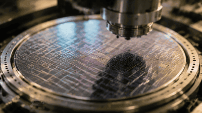
Wafer level packaging works on round silicon wafers, which is convenient because the entire semiconductor industry is already built around wafer processing. Redistribution layers, molding, passivation, and bumping can all happen while the die remains in wafer form, before singulation. That makes WLP a natural extension of wafer fabrication, especially for smaller packages or single-die devices.
Panel level packaging shifts the action to rectangular or square panels. Instead of a circular wafer, the process uses a larger panel format that more closely resembles flat-panel display or substrate manufacturing. In theory, that means better material utilization, more packages per run, and lower cost at scale. In practice, it also means new equipment, new process control challenges, and a different set of yield headaches.
The real question is not whether one is “better” in the abstract. It is where each one wins economically and how well each supports heterogeneous integration.
Why Cost Matters So Much

In advanced packaging, cost is never just a line item. It is often the deciding factor in whether a packaging technology moves from pilot production to broad commercial adoption. A method can be technically impressive and still lose if the manufacturing flow is too expensive, too slow, or too risky.
That matters because advanced packaging is no longer reserved for niche products. AI chips, mobile processors, automotive devices, networking parts, and consumer modules are all asking for more integration at lower cost. Each of these markets has a different tolerance for package cost, and each market pressures PLP and WLP in different ways.
For high-end AI or HPC packages, the cost of packaging may be justified by the value of the system. For mobile or consumer devices, however, a few cents or a small percentage difference can make or break a design. That is why the cost battle between PLP and WLP is so intense: the market is large, diverse, and extremely price sensitive.
Wafer Level Packaging: The Mature Workhorse
WLP has a head start because it fits naturally into the existing wafer ecosystem. Many of the tools, materials, and process flows already exist, and the industry has spent years refining them. That maturity creates several advantages:
- Lower process risk. The industry understands wafer handling, alignment, and singulation well.
- Established supply chain. Materials, metrology, and equipment are widely available.
- Good fit for compact devices. Small dies and low-profile packages work especially well in WLP flows.
- Strong qualification history. WLP is well understood in many consumer and mobile applications.
This makes WLP especially attractive for high-volume, single-die or relatively simple multi-die designs. If the package does not need extremely large routing area, and if the die size fits within the wafer-level process window, WLP can be very cost-effective. The circular wafer format also minimizes the need for new capital investment compared with panel-based alternatives.
But WLP has limits. The wafer diameter constrains the number and size of packages that can be processed at once. As packages grow larger or more complex, edge losses and utilization inefficiencies become more visible. In other words, WLP is efficient until it isn’t.
Panel Level Packaging: The Scale Play
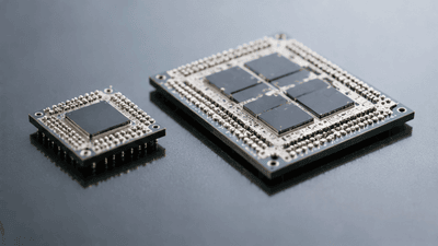
PLP’s big selling point is scale. A panel can hold more packages than a wafer, and rectangular panels can use material more efficiently than round wafers, at least in theory. This is particularly attractive for fan-out and system-in-package applications where the package area is larger than what WLP handles comfortably.
PLP also fits well with the direction of heterogeneous integration. As packages start integrating more chiplets, passives, memory, and interconnect layers, the available real estate matters. Larger panels can support more complex routing, bigger package outlines, and potentially lower manufacturing cost per unit if yields and equipment throughput are good enough.
The attraction is easy to understand:
- More packages per process run.
- Better material utilization from rectangular form factors.
- Potentially lower cost per package in high-volume production.
- More flexibility for larger fan-out and SiP assemblies.
That is the promise. The catch is that panel processes are much younger than wafer processes, and that means higher risk in yield, warpage, handling, and tool maturity.
Where the Cost Battle Is Won or Lost
The PLP versus WLP cost battle is not decided by a single factor. It is a stack of trade-offs. Some of them favor PLP, some favor WLP, and many depend on the package type itself.
1. Equipment Cost and Throughput
PLP often requires new equipment or major tool modifications. That means higher upfront capital expenditure, longer qualification cycles, and more process tuning. WLP can often leverage mature wafer tools and workflows, which lowers the barrier to entry.
However, once PLP tools are mature, the larger panel format can deliver excellent throughput. If a line can process more units per run and maintain good yield, the cost per package may drop significantly. This is where PLP tries to win: not on day one, but over time, as scale and learning improve.
2. Material Utilization
Round wafers are inherently inefficient for rectangular package layouts. If the final package format is large or rectangular, panel-based processing can make better use of the available area. That can reduce waste and improve the economics of fan-out structures, especially for system-in-package designs with multiple dies or large redistribution areas.
WLP still works very well when the package is compact and the circular format matches the product shape. But once the package grows or becomes more irregular, the panel starts to look more attractive.
3. Yield and Warpage
This is where the battle gets real. PLP’s larger format can improve area utilization, but it also creates bigger mechanical challenges. Warpage, stress, and panel flatness become major yield factors. Even small distortions can disrupt fine-pitch routing and die placement.
WLP benefits from a more mature and controlled process window. The industry has spent years reducing defects and improving handling on wafers. PLP is catching up, but yield variability remains one of its biggest economic risks. A high-capacity panel line with poor yield can quickly become more expensive than a slower wafer line with stable output.
4. Design Flexibility
PLP has an edge when package size and heterogeneity increase. Larger panels give designers more room to arrange chiplets, passives, and redistribution layers. That flexibility can be very valuable in advanced encapsulation and heterogeneous integration, where the goal is often to combine several functions in one package.
WLP is better suited to compact devices and simpler layouts. If the design is small and the routing needs are modest, WLP’s maturity and efficiency can outweigh PLP’s scale advantage.
Heterogeneous Integration Changes the Equation
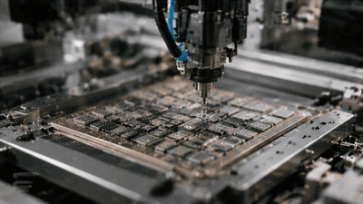
The rise of heterogeneous integration changes how both PLP and WLP should be evaluated. In a world of chiplets, memory stacks, RF front ends, power modules, and embedded passives, the package is no longer a passive shell. It is the system. That makes integration density more important than ever.
PLP tends to shine when the package must host multiple functions across a larger footprint. That makes it attractive for:
- System-in-package modules.
- Multi-die consumer or automotive devices.
- Large fan-out structures with multiple chiplets.
WLP, meanwhile, is often ideal for smaller heterogeneous assemblies where the die count is limited and the package size remains manageable. RF modules, sensors, and power management devices often benefit from WLP’s thinner profile and mature process economics.
In other words, heterogeneous integration does not crown a universal winner. It makes the decision more application-specific. The more integration and package area you need, the more appealing PLP becomes. The more compact and mature the product, the more WLP retains its edge.
Cost Curves Are Not Linear
A mistake often made in this debate is assuming that PLP simply becomes cheaper because panels are larger. The reality is more complicated. Cost curves depend on:
- Yield per process step.
- Tool utilization and uptime.
- Material waste.
- Rework and scrap rates.
- Package size and complexity.
That means a PLP line can outperform WLP for one package type and lose for another. Small fan-out devices might remain more economical on wafers, while larger system-in-package modules benefit from panels. The break-even point is not fixed; it moves with technology maturity, volume, and the specific design.
This is why manufacturers approach PLP carefully. They are not trying to replace WLP everywhere. They are trying to find the application zones where panel economics are strong enough to justify the new process flow.
Thermal and Mechanical Implications
Advanced packaging is not just about cost per package. Thermal and mechanical behavior also matter because they affect yield, reliability, and field performance. PLP and WLP both have to contend with these issues, but they do so differently.
PLP’s larger format can complicate warpage and make handling more difficult. However, it also opens more options for structural design and interconnect placement. WLP generally benefits from a more controlled and mature mechanical environment, but it can be less flexible when the package must stretch in size or support many connections.
For heterogeneous integration, this matters because the thermal and mechanical demands rise as more dies are placed into a single module. A larger PLP structure may be better suited to spreading and routing around those demands, provided the manufacturing process can keep up. WLP is more comfortable when the package stays within the smaller, well-trodden regime.
Who Wins Where?
A practical way to think about the PLP versus WLP cost battle is by application class:
- Mobile and consumer devices. WLP remains very strong, especially for compact, cost-sensitive packages.
- RF, sensor, and power modules. WLP is still highly competitive, though PLP may gain ground as integration complexity rises.
- Automotive and industrial SiP. PLP can become attractive when package size and integration density increase.
- Advanced heterogeneous systems. PLP may win for larger modules with multiple dies and more complex routing needs.
This does not mean one technology will displace the other. More likely, they will coexist, each occupying a different cost-performance zone.
The Road Ahead
PLP is still in a second-wave phase of adoption, where the economic case is getting stronger but engineering reality still matters a lot. If yields improve, warpage control gets better, and panel equipment matures, PLP could unlock real cost advantages in high-volume heterogeneous integration. If not, WLP will continue to dominate compact and mature applications where its process stability and low risk remain hard to beat.
Over the next few years, the market will likely refine this division of labor. WLP will stay strong where miniaturization and maturity matter most. PLP will expand where system complexity, package size, and material utilization make panel processing attractive. The battle will not end with a single winner. It will end with a clearer map of where each technology belongs.
Conclusion
The cost battle between panel level packaging and wafer level packaging is really a story about matching process architecture to product needs. WLP has the advantage of maturity, proven yield, and a well-established supply chain. PLP has the promise of better scale, more flexibility, and lower cost in the right applications. In advanced packaging and heterogeneous integration, those differences matter more than ever.
What makes this contest so important is that the package itself is now part of the system design. As chiplets, memory, RF, and power functions come together in tighter spaces, the choice between PLP and WLP becomes a strategic decision about cost, performance, and manufacturability. The winner is not the technology with the loudest hype. It is the one that best fits the architecture, the volume, and the economics of the product being built.
That is why the PLP versus WLP debate is likely to remain a defining conversation in advanced packaging for years to come.





